The UK National Ion Beam Centre
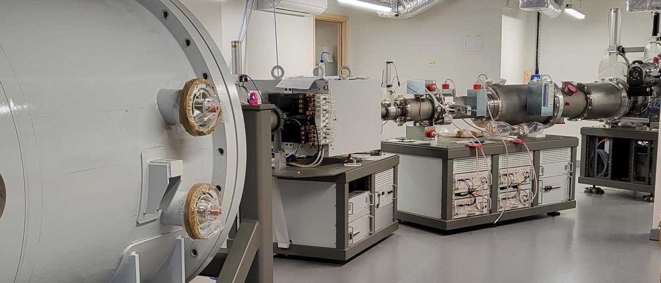
The EPSRC UK National Ion Beam Centre (UKNIBC) provides a single point of access for the UK research community to world-leading ion beam modification and analysis infrastructure and expertise.
It is a collaborative delivery partnership between facilities at:
Providing Ion Beam Facilities to Academia and Industry